• home

Precision Full Wave Ac Dc Converter Circuit Diagram

A dc level is produced that corresponds to the ac input rms value (if sine wave), -i set the gain of IC2 to 1.11. This factor is the average-to-rms conversion factor. IC1 and IC2 act as a full-wave rectifier circuit, with Dl and D2. 

Precision Full-Wave Ac/Dc Converter Circuit Diagram


Precision Full-Wave Ac/Dc Converter Circuit Diagram

LED Driver Circuit Using CAT3603

CAT3603 is a three channel charge pump LED driver IC from Catalyst Semiconductors that can be operated in either LDO mode or fractional mode. The IC can deliver 30mA per channel and can be operated from an input voltage range of 3 to 5.5V DC. CAT3063 has a quiescent current as low as 0.1uA and this makes it suitable for battery powered applications. The operating frequency is 1Mhz which makes it possible to use small capacitors.

LED Driver Circuit Diagram Using CAT3603

Another features are soft start, current limiting, high efficiency (90%) and short circuit protection. Applications of this IC are hand held devices, LCD back lights , LED lighting gadgets etc. The output current can be programmed using an external resistor connected between the RSET (pin 4) and ground.

Charge pump:


Charge pump is a DC to DC converter circuit that uses capacitors as the energy storage component for creating an output voltage that is either higher or lower than the input voltage. A switching circuit (using BJTs or MOSFETs) is used for connecting and disconnecting the voltages from the storage capacitor.

The switching frequency is usually in the kilo or MHz range. The output voltage will be a pulsed one and it is smoothed using an output filter capacitor. Charge pump circuits can double, triple, quadruple, multiply or scale any given voltage. In theory, a charge pump can generate any desired voltage.

CAT3063 LED driver circuit.


The circuit diagram of a three channel LED driver circuit using CAT3063 is shown below (Fig 1). C4 is an input filter capacitor. R1 is the resistor used for programming the output current. C3 is the output filter capacitor. C1 and C2 are the storage capacitors of the internal charge pump circuit. A logic high at pin 5 will enable the IC and a logic low on the same pin will drive the IC into shutdown mode.

In the shutdown mode, the quiescent current is almost equal to zero. With the used value of R1, the LED current per channel will be 25mA. When powered up the CAT6063 operates in 1X mode i.e, the output voltage will be equal to the input voltage. If this output voltage is enough to regulate the current through all LEDs, the IC remains 1X mode.

If the output voltage is not sufficient enough to regulate the desired current through the LEDs, the device automatically switches to the 1.5X mode where the output voltage is 1.5 times the input voltage. This process is repeated when ever the IC is powered up or awaken from shutdown mode.

Selection of R1 is shown in the table below.


LED current (mA) R1 (kilo ohm)
1 649
5 287
10 102
15 49.9
20 32.4
25 23.7
30 15.4

Notes.


CAT6063 is not suitable for resistive loads.
Unused LED output channels must be connected to Vout pin. They cannot be left floating.
All capacitors are ceramic capacitors.
Dimming of the LEds can be achieved by using a DC voltage for setting the pin4 (RSET) current or by driving the pin5 (EN) using a PWM signal.
There is an exposed pad beneath the IC and it should soldered to the ground plane of the PCB for improved thermal performance.
Supply voltage should not exceed 6V DC.
Total output current should not exceed 120mA.

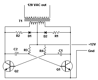
Simple Inverter Circuit Diagram

Have you ever wanted to run a TV, stereo or other appliance while on the road or camping? Well, this inverter should solve that problem. It takes 12 VDC and steps it up to 120 VAC. The wattage depends on which tansistors you use for Q1 and Q2, as well as how "big" a transformer you use for T1. The inverter can be constructed to supply anywhere from 1 to 1000 (1 KW) watts.

Simple Inverter Circuit Diagram

Simple Inverter Circuit Diagram

Parts:
C1, C2 68 uf, 25 V Tantalum Capacitor
R1, R2 10 Ohm, 5 Watt Resistor
R3, R4 180 Ohm, 1 Watt Resistor
D1, D2 HEP 154 Silicon Diode
Q1, Q2 2N3055 NPN Transistor (see "Notes")
T1 24V, Center Tapped Transformer (see "Notes")
MISC Wire, Case, Receptical (For Output)

Notes:
1. Q1 and Q2, as well as T1, determine how much wattage the inverter can supply. With Q1,Q2=2N3055 and T1= 15 A, the inverter can supply about 300 watts. Larger transformers and more powerful transistors can be substituted for T1, Q1 and Q2 for more power.

2. The easiest and least expensive way to get a large T1 is to re-wind an old microwave transformer. These transformers are rated at about 1KW and are perfect. Go to a local TV repair shop and dig through the dumpster until you get the largest microwave you can find. The bigger the microwave the bigger transformer. Remove the transformer, being careful not to touch the large high voltage capacitor that might still be charged. If you want, you can test the transformer, but they are usually still good. Now, remove the old 2000 V secondary, being careful not to damage the primary. Leave the primary in tact. Now, wind on 12 turns of wire, twist a loop (center tap), and wind on 12 more turns. The guage of the wire will depend on how much current you plan to have the transformer supply. Enamel covered magnet wire works great for this. Now secure the windings with tape. Thats all there is to it. Remember to use high current transistors for Q1 and Q2. The 2N3055s in the parts list can only handle 15 amps each.

3. Remember, when operating at high wattages, this circuit draws huge amounts of current. Dont let your battery go dead :-).

4. Since this project produces 120 VAC, you must include a fuse and build the project in a case.

5. You must use tantalum capacitors for C1 and C2. Regular electrolytics will overheat and explode. And yes, 68uF is the correct value. There are no substitutions.

6. This circuit can be tricky to get going. Differences in transformers, transistors, parts substitutions or anything else not on this page may cause it to not function.

Audio Booster Circuit

Small and portable unit, Can be built on a veroboard

The amplifiers gain is nominally 20 dB. Its frequency response is determined primarily by the value of just a few components-primarily C1 and R1. The values of the schematic diagram provide a response of ±3.0 dB from about 120 Hz to better than 20,000 Hz.Actually, the frequency response is ruler flat from about 170 Hz to well over 20,000 Hz; its the low end that deviates from a flat frequency response.

The low ends roll-off is primarily a function of capacitor C1(since RIs resistive value is fixed). If C1s value is changed to 0.1 pF, the low ends comer frequency-the frequency at which the low-end roll-off starts-is reduced to about 70 Hz. If you need an even deeper low-end roll-off, change C1 to a 1.0 pF capacitor; if its an electrolytic type, make certain that its installed into the circuit with the correct polarity, with the positive terminal connected to Q1s base terminal.

Circuit Diagram:

Audio_Booster_Circuit Diagram Audio Booster Circuit Diagram

Parts Description
P1 100K
R1 47K
R2 470K
R3 10K
R4 560R
R5 270R
C1 0.1uF-25v
C2 3.3uF-25v
C3 470uF-25V
D1 5mm. Red Led
B1 9v Battery
J1 RCA Audio Input Socket
J2 RCA Audio Output Socket
S1 On-Off Switch


Source :www.extremecircuits.net

12 V Bidirectional Motor Control Circuit

This simple circuit drives DC motors with a maximum current of 1 A and can be built with readily available components.The output voltage is adjustable between 0 and 14 V and the polarity can be changed so that not only motor speed but also rotation direction can be adjusted by turning a knob.
The circuit is also ideal as a controller for a DC model railway or small low voltage hobby tool. Power for the circuit is supplied by a 18 V mains transformer rated at 1.5 A. Diodes D1to D4 rectify the supply and capacitor C1 provides smoothing to give a DC output voltage of around 24 V. A classic ‘H’ bridge configuration is made up with transistors T1/T3 and T2/T4. Transistors T5 and T6 together with resistors R7 and R8 provide the current sense and limiting mechanism. The maximum output current limit can be changed from 1 A by using different value resistors for R7 and R8: IOUT = 0.6 V / R where R gives the value for R7 and R8. For increased current limit the mains transformer and diodes will need to be changed to cope with the extra current as well as the four transistors used in the bridge configuration.
Circuit diagram:
Motor speed control and direction is controlled by a twin-ganged linear pot (P1). The two tracks of P1 together with R1/R2 and R3/R4 form two adjustable potential divider networks. Wiring to the track ends are reversed so that as the pot is turned the output voltage of one potential divider increases while the other decreases and vice versa.
In the midway position both dividers are at the same voltage so there is no potential difference and the motor is stationary. As the pot is rotated the potential difference across the motor increases and it runs faster. The voltage drop across D5 and D6 is equal to the forward voltage drop VBE of the bridge transistors and ensures that the motor does not oscillate in the off position with the pot at its mid point.
Author :Christian Tavernier

Automatic Loudness Control Circuit

This is a simple design for automatic loudness control in audio. A simple approach to this problem can be done inserting a circuit in the preamplifier stage, capable of varying automatically the frequency response of the entire audio chain in respect to the position of the control knob, in order to keep ideal listening conditions under different listening levels. This is a figure of the circuit.


The circuit is shown with SW1 in the "Control-flat" position, i.e. without the Automatic Loudness Control. In this position the circuit acts as a linear preamplifier stage, with the voltage gain set by means of Trimmer R7. Switching SW1 in the opposite position the circuit becomes an Automatic Loudness Control and its frequency response varies in respect to the position of the control knob by the amount shown in the table below. C1 boosts the low frequencies and C4 boosts the higher ones. Maximum boost at low frequencies is limited by R2; R5 do the same at high frequencies.

This is a list component that must using for built the circuit.
P1 10K Linear Potentiometer (Dual-gang for stereo)

R1, R6, R8 100K 1/4W Resistors
R2 27K 1/4W Resistor
R3, R5 1K 1/4W Resistors
R4 1M 1/4W Resistor
R7 20K 1/2W Trimmer Cermet

C1 100nF/63V
C2 47nF/63V
C3 470nF/63V
C4 15nF/63V
C5, C9 1µF/63V
C6, C8 47µF/63V
C7 100pF/63V

IC1 TL072 Dual BIFET Op Amp

SW1 DPDT Switch (four poles for stereo)

Bipolar Power supply for Battery Instruments Circuit Diagram

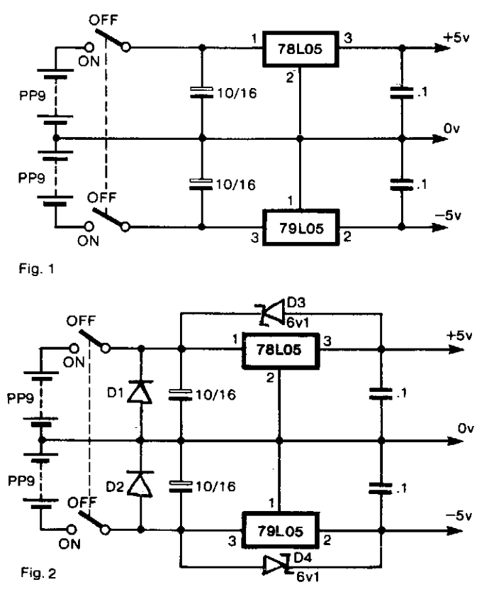
Bipolar Power supply for Battery Instruments Circuit Diagram. To generate regulated ± 5-V supplies from a pair of dry batteries, the circuit of Fig. 1 is commonly used. In order to give protection from inadvertent reverse connection of a battery, a diode in series with each battery would produce an unacceptable voltage drop. The more effective approach is to fit diodes Dl and D2 as shown in Fig. 2, in parallel with each battery. 

When the supply is switched off, there is the risk of a reverse bias being applied across the regulators, if there is significant inductance or capacitance in the load circuit. Diodes across the regulators prevent damage. When the power supply is switched on, the two switches do not act in unison. There is a probability that one or the other regulators will be latched hard off by the other. To prevent this, D3 and D4 are Zener diodes so that ± 5-V rails are pulled up by the batteries until the regulators establish the correct levels.

 Bipolar Power supply for Battery Instruments Circuit Diagram


Bipolar Power supply for Battery Instruments Circuit Diagram

Build a Instrumentation Amplifier Circuit Diagram

How Build a Instrumentation Amplifier . Three-amplifier circuit consumes only 135 /tW of power from a ±1 V power supply. With a gain of 101, the instrumentation amplifier is ideal in sensor interface and biomedical preamplifier applications . The first stage provides all of the gain while the second stage is used to. provide common mode rejection and double-ended to single-ended conversion .

Build a Instrumentation Amplifier Circuit Diagram

Build a Instrumentation Amplifier Circuit Diagram


Audio Variable Filter Circuit Diagram

The filter produces three outputs: high-pass, bandpass, and low-pass. Frequency is linearly proportional to the gain of the two integrators. Two CA3080s, (IC2, 4) provide the variable gain, the resonant frequency being proportional to the current ^. Using 741 op amps for IC3a control range of 100 to 1, (resonant frequency) can be obtained.If CA3140s are used instead of 741s then this range can be extended to nearly 10,000 to 1.

 Audio Variable Filter Circuit Diagram

Audio Variable Filter Circuit Diagram

Very Simple Bench Amplifier circuit and explanation

A small 325mW amplifier with a voltage gain of 200 that can be used as a bench amplifier, signal tracer or used to amplify the output from personal radios, etc. The circuit is based on the National Semiconductor LM386 amplifier. In the diagram above, the LM386 forms a complete non-inverting amplifier with voltage gain of x200. A datasheet in PDF format can be downloaded from the National Semiconductor website. The IC is available in an 8 pin DIL package and several versions are available; the LM386N-1 which has 325mW output into an 8 ohm load, the Lm386N-3 which has 700mW output and the LM386N-4 which offers 1000mW output. all versions work in this circuit. The gain of the Lm386 can be controlled by the capacitor across pins 1 and 8. With the 10u cap shown above, voltage gain is 200, omitting this capacitor and the gain of the amplifier is 20.

Finished project:
Circuit diagram:
Bench Amplifier Circuit Diagram

The IC works from 4 to 12Volts DC, 12Volt being the maximum recommended value. The internal input impedance of the amplifier is 50K, this is shunted with a 22k log potentiometer so input impedance in this circuit will be lower at about 15k. The input is DC coupled so care must be taken not to amplify any DC from the preceeding circuit, otherwise the loudspeaker may be damaged. A coupling capacitor may included in series with the 22k control to prevent this from happening.

Samsung Galaxy S4 Circuit Application


Samsung Galaxy S4 Circuit Application

Anti Theft System Alarm Circuit Wiring Diagramcircuit Schematic

Wiring Diagram on Left Headlight 2 Left Parking Light 3 Right Parking Light 4 Right
Left Headlight 2 Left Parking Light 3 Right Parking Light 4 Right.


Wiring Diagram on Ktm 250 525 Sx  Mxc  Exc Electrical System And Wiring Diagram
Ktm 250 525 Sx Mxc Exc Electrical System And Wiring Diagram.


Wiring Diagram on Wiring Diagram Here   Page 1 And Page 2     Source  Autolib Diakom
Wiring Diagram Here Page 1 And Page 2 Source Autolib Diakom.


Wiring Diagram on System And Wiring Diagram Here  60 Pages Of Pdf File Docs
System And Wiring Diagram Here 60 Pages Of Pdf File Docs.


Wiring Diagram on The Following Schematic Shows A Typical Diagram Schematic Of Polaris
The Following Schematic Shows A Typical Diagram Schematic Of Polaris.


Wiring Diagram on Anti Theft System And Alarm Circuit Wiring Diagram   Circuit Schematic
Anti Theft System And Alarm Circuit Wiring Diagram Circuit Schematic.


Wiring Diagram on Honda Accord Coupe   94 Fan Controls Circuit And Wiring Diagram
Honda Accord Coupe 94 Fan Controls Circuit And Wiring Diagram.


Wiring Diagram on Cassette   Cd And 6 Speakers Audio System Wiring   Circuit Schematic
Cassette Cd And 6 Speakers Audio System Wiring Circuit Schematic.


Wiring Diagram on Ford Factory Stereo Radio Wiring Harness 1996 1997   Ebay
Ford Factory Stereo Radio Wiring Harness 1996 1997 Ebay.


Wiring Diagram on Jeep Grand Cherokee Radio Adaptor Wiring Harness   Circuit Schematic
Jeep Grand Cherokee Radio Adaptor Wiring Harness Circuit Schematic.


Human Reaction Checker Circuit

This is wonderful circuit.by using this circuit you can measure whether you have good reactions or not because If you dont have speed reactions you are unable to get decisions quickly.Just think you are driving your vehicle at once a person appeared in front of your vehicle.at that situation you must have quick reaction to stop your vehicle.This circuit allow you to check it.If it is weak by practicing with this circuit you can improve it.

Here this LED blinks every 1.5s.But the light will appear only for 0.1s within that short period you must try to press the button.try this

5 to 500 feet transmitter circuit diagram

This is so useful circuit because this circuit can transmit signals 5 feet to 500 feet.Here I have used common transistor 2N5225 If you are unable to find this you can use any general purpose transistor.

Note
# About L1 is mentioned on the picture
# This circuit operates with 9V DC
# use 5cm wire as an antenna

15dB UHF TV Antenna Booster Circuit

15dB UHF TV Antenna Booster Circuit15dB UHF TV Antenna Booster Circuit

This is an UHF bandage TV antenna preamplifier circuit With 15dB accretion to body easily. It is formed based on BF180 UHF Transistor. The aboriginal date is an bandage canyon clarify complete by the C1, CV1, L1, L4, C7 and C3, the additional date is a base-common voltage amplifier with low ascribe impedance to match. Body the L1 ~ L4 as air amount braid to access aerial Q-Factor. After assembling, backpack it into a able brownish box and affix the arena of the ambit to the box to abate babble effect.

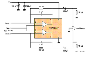
TDA1308T Headphone amplifier circuit

TDA1308T Headphone amplifier circuit 
TDA1308T Headphone amplifier circuit

Battery eliminator circuit


Description.
Here
is the circuit diagram of a battery eliminator circuit that can be
used as a replacement for 9V PP3 batteries. The circuit given here can
be used to power any device that operates from a 9V battery. The
transformer T1 steps down the mains voltage and bridge D1 performs the
job of rectification. Capacitor C1 is a filter. IC LM317T is the
regulator here. The value of R1, R2 and R3 are so selected that the
output voltage of IC1 will be steady 9 volts.
Circuit diagram.
battery eliminator circuit
Notes.
  • Assemble the circuit on a good quality PCB.
  • Transformer T1 can be a 230V primary, 9V secondary, 1.5A step down transformer.
  • If 1A Bridge is not available, then make one using four 1N 4007 diodes.
  • Do not connect loads that consume more than 1.5A to this circuit.
  • A heat sink is recommended for IC1.

10 Watt Stereo Amplifier Circuit Using TDA2009A


This is a design circuit for amplifier. This amplifier circuit has a power of 10 watts. This amplifier circuit is very suitable to apply to your car audio. This amplifier is using IC TDA2009A, as amplifier power. To avoid excessive heat in the IC using some heat sink compound between the heat sink & the IC. C1 & C2 is the input coupling capacitor and blocks DC, as well as C10 & C11 which is the output capacitor Kopel, and C6 & C7 which blocks the DC from the feedback loop. R1/R2 (and R3/R4) set the level of feedback. This is the figure of the circuit.


Get together with 1 (R1/R2) = 68 or 37 dB. C8/R5 (and C9/R6) provides high frequency stability where loudspeaker inductive reactance load can become excessive. C4 and C5 provide power decoupling or filtering. Absolute maximum supply voltage is 28V for the amplifier.

Buffer Circuit

The series is a series of input buffer equal to the output. In this is such a common collector circuit of air-reinforcement = 1. R value attached to restrict the current use is issued. Great value depends on the indication of its components, is usually not installed or flow is maximized in accordance with the op-amp capability.


Buffer circuit here serves to reinforce the clock signal and synchronization for robust enough to be transmitted through a cable with a considerable distance. buffer circuit should have a fairly low output impedance. because the synchronization clock line and this is the track "bus" that is connected to a series of client (branch) in parallel. output current should also be quite large, so as to move a few branches. output buffer in addition to pulse and synchronization signals can also be used as a source of supply.

Buffer circuit using Darlington pairs that have the advantage as expected above. strengthening the buffer is quite high. R base serves as aretaining basis.Vin flow is the input voltage that comes from a series of MMV ( multivibrator). Where active at the level of ± 6V Vin = VCC.

Phono Preamplifier Circuit

Simple circuitry, Passive high-frequency equalization

n recent years, following CDs introduction, vinyl recordings are almost disappeared. Nevertheless, a phono preamplifier is still useful for listening old vinyl discs from a well preserved collection. This simple but efficient circuit devised for cheap moving-magnet cartridges, can be used in connection with the audio power amplifiers shown in these web pages, featuring low noise, good RIAA frequency response curve, low distortion and good high frequency transients behavior due to passive equalization in the 1 to 20 KHz range.

Circuit Diagram:

Phono Preamplifier Circuit diagram Phono Preamplifier Circuit Diagram

Parts:

R1 = 47K
R2 = 100R
R2 = 6.8K
R4 = 68K
R5 = 2.7K-1/2W
R6 = 2.7K-1/2W
R7 = 2.2K
R8 = 39K
C1 = 100uF-25V
C2 = 100uF-25V
C3 = 100uF-25V
C4 = 47nF-63V
C5 = 47nF-63V
D1 = BZX79C18
D2 = BZX79C18
Q1 = BC337
Q2 = BC327
J1 = RCA Jack
IC1 = LM833, Opamp

Notes:

  • R2, R3, R4, R7, R8, C4 & C5 should be low tolerance types.
  • Schematic shows left channel and power supply.
  • For stereo operation R1, R2, R3, R4, R7, R8; J1; C1, C4 & C5 must be doubled.
  • Numbers in parentheses show IC1 right channe

Source : www.redcircuits.com