• home

Hydrophone Booster Amplifier HA2

Hydrophone Booster Amplifier (HA2)

The HP series Hydrophone Booster Amplifier (HA2) amplifies low-level hydrophone signals over a wide range of frequencies. It has a minimum gain of 25dB and an input and output impedance of 50Ω. The HA2 is designed for use with either Precision Acoustics membrane hydrophone or Precision Acoustics HP Series Hydrophone Measurement System, which is shown in Fig 1.

Hydrophone Booster Amplifier 

Alternatively, the HA2 may be used when the acoustic signal is provided by a high output impedance hydrophone, such as a GEC-Marconi membrane device, or a conventional hydrophone. In this instance a BNC/MCX adaptor is used which connects directly to the HP Series Submersible Preamplifier, using it as a buffer amplifier, (i.e. the standard Precision Acoustic HP Series configuration shown in Fig 1 is used, but without the interchangeable probe).

The HA2 amplifier is straightforward to use but the following points should be noted:

  • The output of the amplifier should be correctly terminated in 50Ω before operation.
  • The HA2 amplifier is non-inverting but this is of no consequence when used with the HP Series interchangeable probes as their design takes this into account. However when a submersible preamplifier is used as a high impedance buffer amplifier (as in Fig 2) the system output from the HA2 will be inverted as the HP Series Submersible Preamplifier is inverting.

Before Connecting the unit please read WARNING

To Connect

To  Disconnect

1 Connect Output Load 1 Remove RF Input
2 Apply DC Voltage 2 Remove DC Volts
3 Apply RF Input 3 Remove Load

Specification (HA2 Amplifier Only)

Voltage Gain = 25dB minimum
Bandwidth =  50kHz to 125MHz ±1.0dB
Maximum Output Level = 29dBm for 1dB compression (18.1V pk – pk into 50Ω load)
Input Impedance = Nominal 50Ω
Output Impedance  Nominal 50Ω (VSWR 2:1)
Output Noise Level = Typically 70μV pk – pk (bandwidth 125MHz)
Noise Figure = Typically 10dB
Phase = Non-inverting
Terminations:
Front panel = Input BNC socket BNC Output socket
Rear panel Power Requirements = 28v dc output to supply DC Coupler 100/120/220/240V ac, 50 to 60Hz,
7.5W
Operating Temperature = 0 to 50°C
Size = (90mm × 205mm ×194mm)
Weight = 2.6kg

Copyright : Precision Acoustics March 2004

Headphone Amplifier with IR Communication

This low cost project can be used to reproduce an audio from TV without creating any disturbance from other people. No wire will be used by the circuit between the TV and the headphone because instead of using wires, it utilizes the invisible infrared light for the transmission of audio signals from the TV going to the headphone. The range that can be covered can reach up to 6 meters without using any lens but if required, the range can be made to extend with the use of lenses and reflectors with transmitters and receivers that comprise the IR sensors.

Headphone Amplifier with IR Communication Circuit diagram


Two series connected IR LEDS are being driven by the two-stage transmitter amplifier that uses the IR transmitter. The audio output from TV to the IR transmitter is coupled by using an audio output transformer that is reversely connected. The audio signals are amplified by the transistors BC547 & BD140. These audio signals are received from TV through the low output impedance windings for TV connection of the audio transformer while high impedance for IR transmitter connection.

A 9V source can power the IR transmitter with the LED functioning as power-on indicator.

Build a Instrumentation Amplifier Circuit Diagram

How Build a Instrumentation Amplifier . Three-amplifier circuit consumes only 135 /tW of power from a ±1 V power supply. With a gain of 101, the instrumentation amplifier is ideal in sensor interface and biomedical preamplifier applications . The first stage provides all of the gain while the second stage is used to. provide common mode rejection and double-ended to single-ended conversion .

Build a Instrumentation Amplifier Circuit Diagram

Build a Instrumentation Amplifier Circuit Diagram


Very Simple Bench Amplifier circuit and explanation

A small 325mW amplifier with a voltage gain of 200 that can be used as a bench amplifier, signal tracer or used to amplify the output from personal radios, etc. The circuit is based on the National Semiconductor LM386 amplifier. In the diagram above, the LM386 forms a complete non-inverting amplifier with voltage gain of x200. A datasheet in PDF format can be downloaded from the National Semiconductor website. The IC is available in an 8 pin DIL package and several versions are available; the LM386N-1 which has 325mW output into an 8 ohm load, the Lm386N-3 which has 700mW output and the LM386N-4 which offers 1000mW output. all versions work in this circuit. The gain of the Lm386 can be controlled by the capacitor across pins 1 and 8. With the 10u cap shown above, voltage gain is 200, omitting this capacitor and the gain of the amplifier is 20.

Finished project:
Circuit diagram:
Bench Amplifier Circuit Diagram

The IC works from 4 to 12Volts DC, 12Volt being the maximum recommended value. The internal input impedance of the amplifier is 50K, this is shunted with a 22k log potentiometer so input impedance in this circuit will be lower at about 15k. The input is DC coupled so care must be taken not to amplify any DC from the preceeding circuit, otherwise the loudspeaker may be damaged. A coupling capacitor may included in series with the 22k control to prevent this from happening.

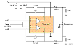
TDA1308T Headphone amplifier circuit

TDA1308T Headphone amplifier circuit 
TDA1308T Headphone amplifier circuit

STK4050 STK4046 Power Amplifier

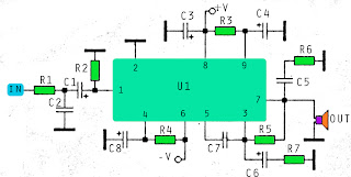
Amplifier circuit with IC STK is tough and good quality. In this article an amplifier circuit with IC STK another base. Power "Amplifier 200Watt By STK4050" is an audio amplifier of the STK family with 200Watt power. To create a power amplifier with the STK4050 IC is not require many external components.


Power Amplifier uses symmetric 30Volt power supply system. Power Amplifier With this STK4050 can reproduce the power 200 Watts at 8 Ohm load spaker. In making Power Amplifier 200Watt With this STK4050 do not forget to provide adequate heat sink for the IC STK 4050 in order to avoid overheating.


Schematics Amplifier STK4050-STK4046


PCB Layout Amplifier

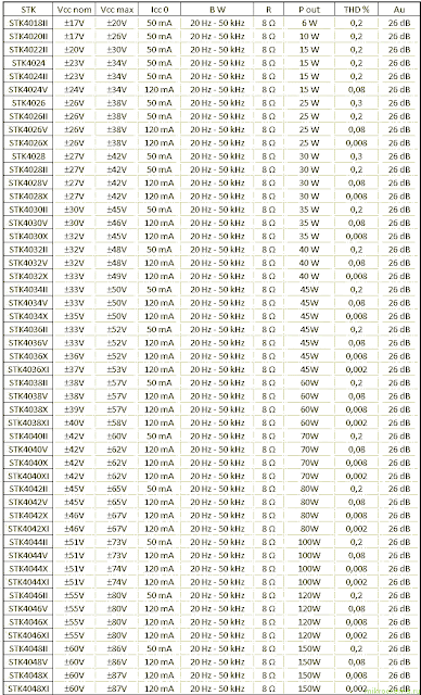
Series Power Supply for Power Amplifier 200Watt By STK4050 been displayed in one image with a series of "Power Amplifier" 200Watt With STK4050 above. IC STK 4050 in this series there are several types on the market including STK4050II, STK4050V and STK4050.

And below is a list of STK ICs are used for a good quality amplifier.

Datasheet STK IC Amplifier

10 Watt Stereo Amplifier Circuit Using TDA2009A


This is a design circuit for amplifier. This amplifier circuit has a power of 10 watts. This amplifier circuit is very suitable to apply to your car audio. This amplifier is using IC TDA2009A, as amplifier power. To avoid excessive heat in the IC using some heat sink compound between the heat sink & the IC. C1 & C2 is the input coupling capacitor and blocks DC, as well as C10 & C11 which is the output capacitor Kopel, and C6 & C7 which blocks the DC from the feedback loop. R1/R2 (and R3/R4) set the level of feedback. This is the figure of the circuit.


Get together with 1 (R1/R2) = 68 or 37 dB. C8/R5 (and C9/R6) provides high frequency stability where loudspeaker inductive reactance load can become excessive. C4 and C5 provide power decoupling or filtering. Absolute maximum supply voltage is 28V for the amplifier.

Modular Headphone Amplifier


140mW into 32 Ohm loads, Ultra-low Distortion
Those wanting private listening to their music programme should add this Headphone Amplifier to the Modular Preamplifier chain. The circuit was kept as simple as possible compatibly with a High Quality performance. This goal was achieved by using two NE5532 Op-Amps in a circuit where IC1B is the "master" amplifier wired in the common non-inverting configuration already used in the Control Center Line amplifier. IC1A is the "slave" amplifier and is configured as a unity-gain buffer: parallel amplifiers increase output current capability of the circuit. Two Headphone outputs are provided by J3 and J4.
The ac gain of the amplifier was kept deliberately low because this module is intended to be connected after the Control Center module, which provides the gain sufficient to drive the power amplifier. If you intend to use this Headphone Amplifier as a stand-alone device, a higher ac gain could be necessary in order to cope with a CD player or Tuner output. This is accomplished by lowering the value of R1 to 1K5. In this way an ac gain of 9 is obtained, more than sufficient for the purpose. Contrary to the two 15V positive and negative regulator ICs used in other modules of this preamp, two 9V devices were employed instead. This because the NE5532 automatically limits its output voltage into very low loads as 32 Ohm in such a way that the output amplitude of the amplified signal remains the same, either the circuit is powered at ±9V or ±15V. The choice of a ±9V supply allows less power dissipation and better performance of the amplifier close to the clipping point.
The input socket of this amplifier must be connected to the Main Out socket of the Control Center Module. As this output is usually reserved to drive the power amplifier, a second socket (J2) wired in parallel to J1 is provided for this purpose. As with the other modules of this series, each electronic board can be fitted into a standard enclosure: Hammond extruded aluminum cases are well suited to host the boards of this preamp. In particular, the cases sized 16 x 10.3 x 5.3 cm or 22 x 10.3 x 5.3 cm have a very good look when stacked. See below an example of the possible arrangement of the front and rear panels of this module.
Circuit diagram :
Modular Headphone Amplifier Circuit Diagram
Parts:
P1___________47K Log. Potentiometer (twin concentric-spindle dual gang for stereo)
R1___________4K7 1/4W Resistor
R2___________12K 1/4W Resistor
R3,R4________33R 1/4W Resistors
R5,R6________4R7 1/4W Resistors
C1___________1µF 63V Polyester Capacitor
C2,C5________100nF 63V Polyester Capacitors
C3,C6________22µF 25V Electrolytic Capacitors
C4,C7________2200µF 25V Electrolytic Capacitors
IC1__________NE5532 Low noise Dual Op-amp
IC2__________78L09 9V 100mA Positive Regulator IC
IC3__________79L09 9V 100mA Negative Regulator IC
D1,D2_______1N4002 200V 1A Diodes
J1,J2________RCA audio input sockets
J3,J4________6mm. or 3mm. Stereo Jack sockets
J5___________Mini DC Power Socket
Notes:
  • The circuit diagram shows the Left channel only and the power supply.
  • Some parts are in common to both channels and must not be doubled. These parts are: P1 (if a twin concentric-spindle dual gang potentiometer is used), IC2, IC3, C2, C3, C4, C5, C6, C7, D1, D2, J3, J4 and J5.
  • This module requires an external 15 - 18V ac (100mA minimum) Power Supply Adaptor.
Technical data:
Output power (1KHz sinewave):
32 Ohm: 140mW RMS
Sensitivity:
275mV input for 1V RMS output into 32 Ohm load (31mW)
584mV input for 2.12V RMS output into 32 Ohm load (140mW)
Frequency response @ 2V RMS:
Flat from 15Hz to 23KHz
Total harmonic distortion into 32 Ohm load @ 1KHz:
1V RMS and 2V RMS 0.0012%
Total harmonic distortion into 32 Ohm load @ 10KHz:
1V RMS and 2V RMS 0.0008%

LM317 Simple Audio Amplifier Circuits

You most likely know that LM317 IC is applied as an practical provide regulator, but did you know it can be applied as an audio amplifier? This is a Low power Amplifier LM317 Simple Audio Amplifier Circuit a audio  designed with LM317 that offers a optimum probable 1W audio strength. 
LM317 Simple Audio Amplifier Circuit Diagrams :
LM317 Simple Audio Amplifier Circuits

Utilization a amazing heatsink for the LM317 IC and modify the 5K various resistor so that you have 4.5V on 10Ω resistor (or LM317 pin 2, Vout).

25W Audio Power Amplifier Rise

This audio power amplifier project is based on LM1875 amplifier module from National Semiconductor. It can deliver up to 30W of power using an 8 ohm load & dual 30V DC power supplies. It is designed to operate with maximum outside parts with current limit & thermal shutdown protection features . Other features include high gain, quick slew rate, wide power supply range, giant output voltage swing & high current capability.

Summary of the audio amply-fire features:

  • Low distortion: 0.015%, 1 kHz, 20 W
  • Wide power bandwidth: 70 kHz
  • Wide supply range 16V-60V
  • Up to 30 watts output power
  • Internal output protection diodes
  • Protection for AC & DC short circuits to ground
  • 94 dB ripple rejection
  • Plastic power package TO-220
25V Power Supply

The schematic below shows how the +25V DC & -25V DC are obtained. In order to provide power supply for two stereo amplifiers, a power transformer rating of 80VA with 240V/36V middle tapped secondary winding is used. The secondary output of the transformer is rectified by using 1N5401 diodes together with four electrolytic capacitors to smoother the ripple voltage. A fuse & a varistor are connected at the primary input to protect the circuit against power surge.


Audio Amplifier Module

The +25V & -25V DC power supply are connected to the audio amplifier module through a 2A fuse with the peripheral devices shown in the schematic below. The audio input signal to be amplified is coupled to pin one of LM1875 through the resistor R1 and electrolytic capacitor E5.

The output signal at pin four of LM1875 can be used to directly drive a 8 ohm loudspeaker. Resistor R6 and capacitor C5 prevent-the capacitance developed at the long speaker leads from driving the amplifier in to High Frequency Oscillation.

A heat-sink with a thermal resistance rating of one.4 Cecilius/Watt or better must be used or else the amplifier module will-be cut-off from operation due to the heat that will build up in the coursework of the operation of the amplifier. Take note that the heat sink tab on the IC module is internally connected to the -25V power supply hence it must be isolated from the heat sink by the use of an insulating washer. If this is not done, the negative rail will be shorted to ground.


2 3 Watt Low audio power amplifier

KA2202 , KA2207
These amplifiers using IC KA2202 and KA2207, which has a power output of 2.3 Watt berimpedansi 4 ohms. Minimum supply voltage and maximum 5Volt 20Volt. See schematics and component list below.


Part List 
R1 = 100K
R2 = 56R
R3 = 56R
R4 = 1R
Use 1/4 Watt resistor
10W schematic amplifier with KA2202 , KA2207

C1 = 100uF
C2 = 100uF
C4 = 100uF
C5 = 470uF
C6 = 100nF
C7 = 470pF
C8 = 2,2nF
C9 = 100uF
U1 = KA2202 , KA2207

70W STK amplifier schematic

home amplifier schematics
For this amplifier circuit using three voltage plus, min, and the ground. with a maximum voltage approximately 55Volt DC. And amplifier circuit can use some ic ie IC STK 030, 058, 075, 077, 078, 080, 082, 083, 084, 086. From all the ic I mentioned all of them can be applied to this amplifier circuit. But every ic whether there might be a different maximum voltage or power output, etc.. For this amplifier suitable for use at home, who need a voice soft and tasty. With a maximum output of 70W 8ohm impedance is my take of the highest IC output is STK086.
Part List
R1 = 1K
R2 = 56K
R3 = 100R
R4 = 100R
R5 = 56K
R6 = 4.7R
R7 = 2.7K
C1 = 1uF
C2 = 470pF
C3 = 100uF
C4 = 100uF
C5 = 0.047uF
C6 = 47uF
C7 = 1800pF
C8 = 10uF
IC = STK 030, 058, 075, 077, 078, 080, 082, 083, 084, 086.

14W CLASS A AMPLIFIER USING 2N3055 ELECTRONIC DIAGRAM

14W CLASS A AMPLIFIER USING 2N3055 ELECTRONIC DIAGRAM

Why Class A ? Because , when biased to class A, the transistors are always turned on, always ready to respond instantaneously to an input signal. Class B and Class AB output stages require a microsecond or more to turn on. The Class A operation permits cleaner operation under the high-current slewing conditions that occur when transient audio signal are fed difficult loads. His amplifier is basically simple, as can be seen from the block diagram.

LM1875 – POWER AMPLIFIER 20 WATT

 
The LM1875 is a monolithic power amplifier offering very low distortion and high quality performance for consumer audio applications.

The LM1875 delivers 20 watts into a 4Ω or 8Ω load on ±25V supplies. Using an 8 load and ±30V supplies, over 30 watts of power may be delivered. The amplifier is designed to operate with a minimum of external components. Device overload protection consists of both internal current limit and thermal shutdown.

The LM1875 design takes advantage of advanced circuit techniques and processing to achieve extremely low distortion levels even at high output power levels. Other outstanding features include high gain, fast slew rate and a wide power bandwidth, large output voltage swing, high current capability, and a very wide supply range. The amplifier is internally compensated and stable for gains of 10 or greater.

Features
• Up to 30 watts output power
• AVO typically 90 dB
• Low distortion: 0.015%, 1 kHz, 20 W
• Wide power bandwidth: 70 kHz
• Protection for AC and DC short circuits to ground
• Thermal protection with parole circuit
• High current capability: 4A
• Wide supply range 16V-60V
• Internal output protection diodes
• 94 dB ripple rejection
• Plastic power package TO-220
LM1875 - POWER AMPLIFIER 20 WATT, link

IC LM12 150 Watts high power amplifier


To supply the required voltage to the  amplifier circuit minimum of 7 Volt and a maximum of 24 volts . Incurred sizable ouput for amplifier ic 300 W maximum output.
high power amplifier schematic
Part List :
R1_____________________________________10K
R2_____________________________________10K
R3_____________________________________220K
R4_____________________________________2.2R 2W
C1_____________________________________1uF
C2_____________________________________1000uF
C3_____________________________________68pF
D1_____________________________________BY229
D2_____________________________________BY229
L1_____________________________________4MH
IC1____________________________________LM12