• home

Simple Inverter Circuit Diagram

Have you ever wanted to run a TV, stereo or other appliance while on the road or camping? Well, this inverter should solve that problem. It takes 12 VDC and steps it up to 120 VAC. The wattage depends on which tansistors you use for Q1 and Q2, as well as how "big" a transformer you use for T1. The inverter can be constructed to supply anywhere from 1 to 1000 (1 KW) watts.

Simple Inverter Circuit Diagram
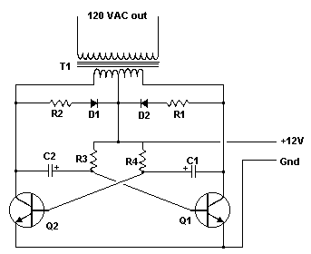
Simple Inverter Circuit Diagram

Parts:
C1, C2 68 uf, 25 V Tantalum Capacitor
R1, R2 10 Ohm, 5 Watt Resistor
R3, R4 180 Ohm, 1 Watt Resistor
D1, D2 HEP 154 Silicon Diode
Q1, Q2 2N3055 NPN Transistor (see "Notes")
T1 24V, Center Tapped Transformer (see "Notes")
MISC Wire, Case, Receptical (For Output)

Notes:
1. Q1 and Q2, as well as T1, determine how much wattage the inverter can supply. With Q1,Q2=2N3055 and T1= 15 A, the inverter can supply about 300 watts. Larger transformers and more powerful transistors can be substituted for T1, Q1 and Q2 for more power.

2. The easiest and least expensive way to get a large T1 is to re-wind an old microwave transformer. These transformers are rated at about 1KW and are perfect. Go to a local TV repair shop and dig through the dumpster until you get the largest microwave you can find. The bigger the microwave the bigger transformer. Remove the transformer, being careful not to touch the large high voltage capacitor that might still be charged. If you want, you can test the transformer, but they are usually still good. Now, remove the old 2000 V secondary, being careful not to damage the primary. Leave the primary in tact. Now, wind on 12 turns of wire, twist a loop (center tap), and wind on 12 more turns. The guage of the wire will depend on how much current you plan to have the transformer supply. Enamel covered magnet wire works great for this. Now secure the windings with tape. Thats all there is to it. Remember to use high current transistors for Q1 and Q2. The 2N3055s in the parts list can only handle 15 amps each.

3. Remember, when operating at high wattages, this circuit draws huge amounts of current. Dont let your battery go dead :-).

4. Since this project produces 120 VAC, you must include a fuse and build the project in a case.

5. You must use tantalum capacitors for C1 and C2. Regular electrolytics will overheat and explode. And yes, 68uF is the correct value. There are no substitutions.

6. This circuit can be tricky to get going. Differences in transformers, transistors, parts substitutions or anything else not on this page may cause it to not function.

Very Simple Bench Amplifier circuit and explanation

A small 325mW amplifier with a voltage gain of 200 that can be used as a bench amplifier, signal tracer or used to amplify the output from personal radios, etc. The circuit is based on the National Semiconductor LM386 amplifier. In the diagram above, the LM386 forms a complete non-inverting amplifier with voltage gain of x200. A datasheet in PDF format can be downloaded from the National Semiconductor website. The IC is available in an 8 pin DIL package and several versions are available; the LM386N-1 which has 325mW output into an 8 ohm load, the Lm386N-3 which has 700mW output and the LM386N-4 which offers 1000mW output. all versions work in this circuit. The gain of the Lm386 can be controlled by the capacitor across pins 1 and 8. With the 10u cap shown above, voltage gain is 200, omitting this capacitor and the gain of the amplifier is 20.

Finished project:
Circuit diagram:
Bench Amplifier Circuit Diagram

The IC works from 4 to 12Volts DC, 12Volt being the maximum recommended value. The internal input impedance of the amplifier is 50K, this is shunted with a 22k log potentiometer so input impedance in this circuit will be lower at about 15k. The input is DC coupled so care must be taken not to amplify any DC from the preceeding circuit, otherwise the loudspeaker may be damaged. A coupling capacitor may included in series with the 22k control to prevent this from happening.

How to make a simple Speaker


Today Im going to tell you how to make a simple speaker.First of all you need a plastic cup,a Magnet,coil.Then turn coil around the magnet turn about 40 turns.Then after fix the magnet middle of the plastic cup.finally connect the wires to the out put of your radio set then you can listen the sound.
Note

# Before you switching on the radio check whether volume controller is in low position or not.Because If not the coil will be burnt.

Simple Car Battery Charger

http://www.electronic-circuits-diagrams.com/psimages/7.gif This very simple circuit uses a transformer ,two diodes , a capacitor and an ammeter.To charge a battery just connect the + and - terminals of the circuit to the corresponding terminals of the battery.When the battery is not charged, the ammeter reading shows 1-3 amps.When the battery is fully charged the ammeter reads Zero or nearly zero, after which the battery should be removed from the charger.

Simple Remote Control Tester

Nearly always when a remote control doesn’t work, the underlying problem is elementary: the unit does not emit light. The cause may be dry solder joints, defective LEDs etc., but also a flat battery (perhaps due to stuck key). The human eye is unable to perceive infra-red light. By contrast, an ordinary photo transistor like the BP103 has no problems working in the infrared spectrum, so in the circuit here it simply biases the BC558 which, in turn, makes LED D1 flash in sympathy with the telegram from the remote control. The preset in the circuit determines the sensitivity.

Simple Remote Control Tester circuit diagram

Simple Ni Cad Battery Charger

This simple charger circuit uses a single transistor as a constant current source. The voltage across the pair of 1N4148 diodes biases the base of the BD140 medium power transistor. The base-emitter voltage of the transistor and the forward voltage drop across the diodes are relatively stable. The charging current is approximately 15mA or 45mA with the switch closed. This suits most 1.5V and 9V rechargeable batteries.


The principle work of the charger is between one batteries with other battery dissociated by packer wall which there is in battery box, mean every space at battery doesnt correlate in consequence electrolyte fluid at every battery nor correlates (partition wall between batteries there shall no which leak).

In one batteries there is arrangement of plate that is some plates for positive pole (between plates dissociated by timber, ebonite or plastics, depends on technology applied) and some plates for negativity pole. Active agent from positive plate made from chocolate tin oxide (PbO2) while active agent from negativity plate is tin (Lead) pore (like sponge). The plates soaked by electrolyte fluid that is sulfate acid (H2SO4).

LM317 Simple Audio Amplifier Circuits

You most likely know that LM317 IC is applied as an practical provide regulator, but did you know it can be applied as an audio amplifier? This is a Low power Amplifier LM317 Simple Audio Amplifier Circuit a audio  designed with LM317 that offers a optimum probable 1W audio strength. 
LM317 Simple Audio Amplifier Circuit Diagrams :
LM317 Simple Audio Amplifier Circuits

Utilization a amazing heatsink for the LM317 IC and modify the 5K various resistor so that you have 4.5V on 10Ω resistor (or LM317 pin 2, Vout).

A Simple yet Effective LED Strobe Light Circuit Explained


You might be quite familiar with strobe lights and should have seen them pretty commonly in parties and discotheques. Although these devices use laser lighta for the generation of the required strobe effect, using high bright LEDs can also be a good alternative, if many of are included. Here we discuss a very simple yet very effective LED strobe light circuit which is in fact more innovative than its commercial counterparts as it produces a chasing effect to lights while implementing the strobing effect simultaneously.


Image Credit - http://www.dinodirect.com/stage-effects-strobe-light-led-ktv-home-decorative-lighting-four-layers.html

Circuit Description:


The circuit is highly innovative and versatile, it actually can be used in many different applications, like in toys, decoration items, as party lights, and in avionics for displaying warning signals from the airplane (tail light probably).

The circuit utilizes the popular IC 4017 for generating the basic chasing or sequencing output through its outputs.


However the above chasing effect becomes a very primary application of the IC and here we are not looking for just a chasing effect, rather we are interested in the strobing pattern which is induced in the circuit by forcing the outputs of the 4017 IC to flash or blink rapidly as it sequences the lights.

To make the IC output strobe, we introduce another IC 4049 and integrate it to the LEDs in the circuit. The IC 4049 basically consists of 6 NOT gate. 

Here two of them are used and configured as an oscillator. Two of the gates are used buffers for facilitating better grounding effect to the LEDs, while the remaining two are used as another oscillator for driving the IC 4017 clock input.

The strobing oscillator and the clocking oscillator can be varied discretely through the respective pots for creating user defined intriguing LED strobe effects.

The LEDs common cathode termination is not connected to its usual position, i.e. to the ground; rather it’s connected to the output of the buffer NOT gates.

The oscillator from the 4049 IC transmits; rapid high and low logic pulses to the buffers which carry forward the response to the LED cathode. When the buffer out is high the LEDs remain shut off during that instant.

However the moment the buffer outputs go low, the LEDs light up and flash rapidly while sequencing, as the LED cathodes now find the ground path through the buffer low output.


Simple VGA to BNC Adapter Converter Circuit

There are monitors which only have three BNC inputs and which use composite synchronization (‘sync on green’). This circuit has been designed with these types of monitor in mind. As can be seen, the circuit has been kept very simple, but it still gives a reasonable performance. The principle of operation is very straightforward. The RGB signals from the VGA connector are fed to three BNC connectors via AC-coupling capacitors. These have been added to stop any direct current from entering the VGA card. A pull-up resistor on the green output provides a DC offset, while a transistor (a BS170 MOSFET) can switch this output to ground. It is possible to get synchronisation problems when the display is extremely bright, with a maximum green component.

In this case the value of R2 should be reduced a little, but this has the side effect that the brightness noticeably decreases and the load on the graphics card increases. To keep the colour balance the same, the resistors for the other two colors (R1 en R3) have to be changed to the same value as R2. An EXOR gate from IC1 (74HC86) combines the separate V-sync and H-sync signals into a composite sync signal. Since the sync in DOS-modes is often inverted compared to the modes commonly used by Windows, the output of IC1a is inverted by IC1b. JP1 can then by used to select the correct operating mode. This jumper can be replaced by a small two-way switch, if required.

VGA-to-BNC Adapter_165 VGA-to-BNC Adapter diagram_165
   parts VGA-to-BNC Adapter_165pcb VGA-to-BNC Adapter_165

This switch should be mounted directly onto the PCB, as any connecting wires will cause a lot of interference. The PCB has been kept as compact as possible, so the circuit can be mounted in a small metal (earthed!) enclosure. With a monitor connected the current consumption will be in the region of 30 mA. A 78L05 voltage regulator provides a stable 5 V, making it possible to use any type of mains adapter, as long as it supplies at least 9 V. Diode D2 provides protection against a reverse polarity.

LED D1 indicates when the supply is present. The circuit should be powered up before connecting it to an active VGA output, as otherwise the sync signals will feed the circuit via the internal protection diodes of IC1, which can be noticed by a dimly lit LED. This is something best avoided.
Resistors:
R1,R2,R3 = 470Ω
R4 = 100Ω
R5 = 3kΩ3
Capacitors:
C1,C3,C5 = 47µF 25V radial
C2,C4,C6,C7,C10 = 100nF ceramic
C8 = 4µF7 63V radial
C9 = 100µF 25V radial
Semiconductors:
D1 = LED, high-efficiency
D2 = 1N4002
T1 = BS170
IC1 = 74HC86
IC2 = 78L05
Miscellaneous:
JP1 = 3-way pinheader with jumper
K1 = 15-way VGA socket (female), PCB mount (angled pins)
K2,K3,K4 = BNC socket (female), PCB mount, 75Ω    . Link

Simple Lighting Surge Protector Circuit

GDT’s are special type of gas filled tubes used for wide range of electronic/electrical circuits for providing protection against lightning and other power surges.  These tubes basically has two electrodes that are kept inside a gas filled closed envelope. In case of electronic applications, the container is mostly ceramic in nature. For high grade electrical applications military tubes are used. The electrical characteristics of this tubes depends on the pressure and composition of gas, and the distance between the two electrodes contained inside. The most commonly used gases in GDT’s are given below.

1) Hydrogen gases
2) Deuterium gases
3) Noble gases
4) Elemental vapors (metals and nonmetals)
5) Other gases
6) Insulating gases
An image of a ceramic discharge tube is shown below. Take a look.

There will be conduction inside the GDT’s due to ionization of gas molecules. Each GDT have a specific voltage and current rating. A simple lightning protector circuit is given below.

Lighting/Surge Protector Circuit

In power lines, usually large amount of voltage is induced (typically very short time with high amplitude) due to lightning (direct or indirect strike) or Transients*
* (Transients caused by other equipments are usually caused by the discharge of stored energy in inductive and capacitive components. Electric motors, such as those used in elevators, heating, air conditioning, refrigeration or other inductive loads, can create a continuous stream of 250V to 1000V transients. DC motor drives, variable speed AC motor drives, DC power supply switching, and portable power tools are other sources of transients.)

Lightning protection circuit:

Simple Lighting Surge Protector Circuit

The basic surge suppression circuit shown below consists of a VDR** (Voltage Dependent Resistor) and gas surge suppressor (GDT) connected in series. The protection circuit is connected between live and mains lead. Normally no current flows through GDT and VDR1. When   the voltage between the terminals is higher than the sum of voltage ratings of GDT and VDR1 (here both GDT UZ470B and VDR S20K250 has 250v 16A rating), current starts to flow through those components. 

If more the voltage rises then more current starts to flow through GDT and VDR1.When the current is normal, the circuit is reset and resumes it’s functioning. Thus the current cannot be raised much over that predetermined value. When the voltage again goes back to normal values G1 and VDR1, the conducting stops and the circuit remains normal.  If the flowing current is more than the specified value of main self-resettable fuse, the fuse will break and the circuit will be protected. After the current is normal, the fuses resets and continue its functioning (protection against short circuit and overload). 

The circuit is designed to protect sensitive electronic devices against overvoltage transients in normal mains voltage and overload/ short circuit. Two neon pilot lamps are also provided with the circuit diagram to show the status of input and load supply.

(**A VDR (Voltage Dependent Resistor) is an electronic component with a “diode-like” nonlinear current–voltage characteristic. The name is a portmanteau of variable resistor.  VDRs are often used to protect circuits against excessive transient voltages by incorporating them into the circuit in such a way that, when triggered, they will shunt the current created by the high voltage away from the sensitive components. A VDR is also known as Voltage Dependent Resistor or VDR. A VDR’s function is to conduct significantly increased current when voltage is excessive.)

Voltage Dependent Resistor

Advantages:

1)      Normal working voltage = 230v AC/DC
2)      Maximum current rating=16A
3)      Cut-off current =16A
4)      Cut-off voltage= >300v R.M.S
5)      Protection against overloads
6)      Protection for short circuit

Applications:

1)      Protection for sensitive components
2)      Protection for motor devices
3)      Telephone line protection
4)      SMPS protection